


PCB Design Mastery – Complete Eagle PCB Design Course from Beginner to Expert

Original price was: ₹4,889.00.₹699.00Current price is: ₹699.00.
🚀 PCB Design Mastery is a complete hands-on course that teaches you how to design professional PCBs using Autodesk Eagle.
You’ll start from zero and learn schematic creation, component libraries, board layout, manual and auto routing, DRC checks, and multi-layer PCB design.
The goal is to make you a job-ready PCB designer who can create boards ready for fabrication and assembly.
This course includes real-world projects, Gerber generation, and design validation.
Taught by Embedded Mastery Academy (JS Rana), it covers everything from basic schematics to complex industrial PCBs – making you a true expert in PCB Design Mastery.
5000 in stock
Welcome to PCB Design Mastery, your step-by-step guide to becoming a professional PCB designer with Autodesk Eagle.
This course is built for absolute beginners who want to learn how to design schematics, route boards, and generate manufacturing files for real production.
By the end, you’ll be able to create single, double, and multi-layer PCBs that meet industrial standards.
⚙️ Course Overview – From Schematic to Fabrication
The PCB Design Mastery course follows a complete design workflow:
Create schematics and annotate components.
Manage symbols and footprints in Eagle libraries.
Convert schematic to board layout and define board shape.
Route signals manually or with the autorouter.
Perform DRC and ERC checks to eliminate errors.
Generate Gerber and BOM files for fabrication.
Once you understand this flow, you can design 2-layer and 4-layer boards like a professional – that’s what PCB Design Mastery is about.
🧩 Detailed Course Curriculum
1. Getting Started with Eagle and PCB Concepts
Understand what a PCB is and why it’s important in electronics.
Install and set up Autodesk Eagle software.
Explore the interface – Schematic Editor, Board Editor, and Control Panel.
Learn how projects are structured and how to save files properly.
2. Schematic Design Fundamentals
Draw electrical schematics using Eagle’s symbols and nets.
Add components from built-in libraries and create connections.
Use labels, buses, and net names for neat circuit layouts.
Check connectivity and prepare the design for conversion to a PCB.
3. Component Libraries and Custom Footprints
Work with Eagle component libraries and add external collections like SparkFun or Adafruit.
Design custom symbols and packages when needed.
Link schematic symbols with board footprints to form complete devices.
Verify component sizes using datasheets and measurements.
4. Board Layout and Layer Setup
Transfer schematic to board layout.
Define board outline, dimensions, and mounting holes.
Configure layers, copper thickness, and clearance rules.
Plan for signals, power planes, and ground paths for best performance.
5. Manual and Auto Routing Techniques
Practice manual routing for critical signals.
Use the Eagle autorouter efficiently to save time.
Understand trace widths, via sizes, and signal separation.
Learn how to route power and ground nets with low noise and low resistance.
6. Design Rule Checks and Validation
Run Electrical Rule Check (ERC) and Design Rule Check (DRC) to catch mistakes.
Fix airwires and unconnected nets automatically.
Inspect trace width violations and clearance errors.
Validate the board like a professional designer – a core habit in PCB Design Mastery.
7. Ground Planes and Thermal Relief
Add copper pours for GND and VCC nets.
Use thermal reliefs to balance heat and soldering ease.
Stitch vias for better current distribution.
Apply EMI/EMC concepts for clean signal performance.
8. Multi-Layer PCB Design
Create and configure layer stack-ups for 4-layer and 6-layer boards.
Design with inner planes for power and ground.
Use blind and buried vias for high-density routing.
Implement impedance control for high-speed signals.
9. Design for Manufacturing and Gerber Files
Generate Gerber, Drill, and Pick-and-Place files for fabrication.
Export Bill of Materials (BOM) for assembly.
Understand DFM principles – minimum trace widths, drill sizes, clearances.
Test your files with online Gerber viewers before sending to PCB manufacturers.
10. Real-World Projects and Case Studies
Design a sensor module, power supply board, or Arduino shield.
Fabricate your own board and verify it after assembly.
Reverse-engineer existing boards to learn industrial techniques.
This hands-on practice cements your learning in PCB Design Mastery.
🎓 Why Choose PCB Design Mastery
✅ No experience required – everything taught step by step.
✅ Practical real-world projects to build confidence.
✅ Covers industrial standards – DRC, BOM, Gerber.
✅ Taught by JS Rana, hardware expert behind 5000+ products.
✅ Lifetime access and a certificate from Embedded Mastery Academy.
🧭 Who Should Join
🎓 Students (B.Tech, Diploma, M.Tech) interested in PCB skills.
⚙️ Working professionals in R&D and hardware development.
👩🔬 Researchers and PhD scholars needing custom PCBs for projects.
💡 Hobbyists who want to fabricate their own boards confidently.
🎓 Explore Our Other Courses
👉 Arduino Mastery – Ultimate Course for Complete Arduino Learning
👉 Electronics Mastery – Complete Course on Core Electronics & Hardware Fundamentals
👉 PCB Design Mastery – Learn Professional Eagle CAD PCB Design Step-by-Step
❓ Frequently Asked Questions
Q1. What is covered in the PCB Design Mastery course?
A. The PCB Design Mastery course covers the entire workflow of PCB design using Autodesk Eagle CAD, including schematic creation, board layout, DRC & ERC checks, routing, and multi-layer design. You’ll master how to design fabrication-ready PCBs for real-world applications.
Q2. Is the PCB Design Mastery course suitable for beginners?
A. Yes, absolutely. This course starts from scratch — perfect for beginners who’ve never used Eagle CAD before. By the end, you’ll design industrial-grade multi-layer PCBs confidently with full understanding of every design step.
Q3. Does the course include practical PCB projects?
A. Yes, this is a 100 % practical course. You’ll design real-world boards such as Arduino shields, sensor modules, and power supply boards. You’ll also generate Gerber files and learn how to get them manufactured using services like JLCPCB or PCBWay.
Q4. What skills will I gain from PCB Design Mastery?
A. You’ll learn to create schematics, manage component libraries, perform manual and auto routing, validate designs with DRC & ERC, generate Gerbers, and apply Design-for-Manufacturing (DFM) principles — skills every hardware engineer must know.
Q5. Do I receive certification after completing the PCB Design Mastery course?
A. Yes ✅. After completing all lessons and projects, you’ll receive a verified certificate from Embedded Mastery Academy by JS Rana, proving your professional competence in Eagle-based PCB design.
🌍 External References
Related products


Electrical Engineering Projects


Electronics Engineering Projects


Army & Defence Innovation Projects
Military Wireless Communication Project – Multi-Team RF Command System
Electronics Engineering Projects
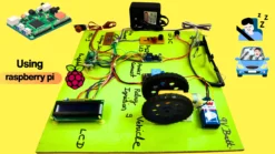
Driver Drowsiness and Alcohol Detection Vehicle Safety System Using Raspberry Pi Pico